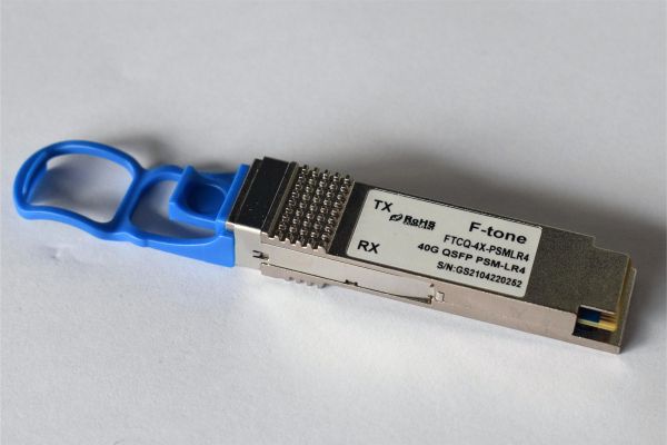
The FTCQ-4X-PSMLR4-GC&FTCQ-4X-PSMLR4I-GC QSFP+ PSM4 optical transceiver is intended for up to 10km reach service with four-lane 10.3125G data rate. It is based on 3.3V DC power supply and operates in the temperature range. It is compliant with QSFP MSA、SFF-8436 and IEEE802.3ba-2018. Digital diagnostic functions are available via I2C interface,and the control functions can be achieved by LVTTL interfaces on the host, mainly including Module Select(ModSelL)、Module Reset(ResetL)、Low Power Mode(LPMode). The transceiver incorporates a four-laser array which is usually DFB 、four-PIN diode array 、an integrated four drivers and TIAs IC separately. The differential AC coupled Tx and Rx data interfaces are CML compatible.
Applications
- 40G BASE Ethernet
- Infiniband EDR interconnects
- Enterprise networking
Features
- MPO-12 optical interface
- Maximum link length upto10km
- Upto 10.3125Gb/s data linksper lane
- +3.3 V power supply
- QSFPMSA compliant package
- Hot Pluggable
- High performance singal modeDML transmitter
- High sensitivity PIN/TIA optical receiver
- Single Mode operation
- Case Operating temperature: 0 to 70ºC, -40to +85 ºC
- Data and Control Interfaces
- Tx DataCML/AC Coupled
- Rx DataCML/AC Coupled
- ModSelL LVTTL
- ResetL LVTTL
- ModPrsL LVTTL
- LPModeLVTTL
- 2-wire I2C communicationbus
- RoHS 6 compliance
Absolute maximum parameters
|
Absolute Maximum Ratings (EXCEEDING THESE RATINGS MAY CAUSE IRREVERSIBLE DAMAGE TO THE DEVICE) |
|||||
|
Parameter |
Symbol |
Min |
Max |
Units |
Notes |
|
Storage Temperature |
Tstg |
-40 |
+95 |
ºC |
Exceeding the absolute maximum ratings may cause irreversible damage to the device. The device is not intended to be operated under the condition of simultaneous absolute maximum rat- ings, which may cause irreversible damage to the device. |
|
Case Operating Temperature |
TO |
0 |
70 |
ºC |
|
|
-40 |
+85 |
||||
|
Relative Humidity - Storage |
RHS |
0 |
95 |
% |
|
|
Relative Humidity - Operating |
RHO |
0 |
85 |
% |
|
|
Supply Voltage |
VCC |
-0.3 |
3.6 |
V |
|
Operating conditions
|
Recommended Operating Conditions |
||||||
|
Parameter |
Symbol |
Min |
Typ |
Max |
Units |
Notes |
|
Case Operating Temperature |
Tcase |
0 |
- |
+70 |
ºC |
|
|
-40 |
- |
+85 |
||||
|
DC Supply Voltage |
VCC |
3.135 |
- |
3.465 |
V |
|
|
Module Supply Current |
Iin |
- |
- |
1060 |
mA |
|
Electrical Characteristics
|
Transmitter Electrical Characteristics |
||||||||
|
Parameter |
Symbol |
Mi |
Typ |
Max |
Units |
Notes |
||
|
Differential Data input Swing |
Vin |
180 |
- |
900 |
mV |
|||
|
Tx Differential Input Impendence |
Zin |
90 |
100 |
110 |
Ω |
|||
|
Tx Differential Output Impendence |
Zout |
45 |
50 |
55 |
Ω |
|||
|
ResetL Disable Voltage |
Vr |
2.0 |
- |
Vcc+0.3 |
V |
|||
|
ResetL Enable Voltage |
VrEN |
0 |
- |
0.8 |
V |
|||
|
ModSelL Disable Voltage |
Vm |
2.0 |
- |
Vcc+0.3 |
V |
|||
|
ModSelL Enable Voltage |
VmEN |
0 |
- |
0.8 |
V |
|||
|
Receiver Electrical Characteristics |
||||||||
|
Parameter |
Symbol |
Min |
Typ |
Max |
Units |
Notes |
||
|
Differential Data Output Swing |
Vout |
180 |
- |
900 |
mV |
|||
|
Rx Differential Output Impendence |
Zout |
90 |
100 |
110 |
Ω |
|||
|
IntL Assert Voltage |
VInt |
VCC-0.5 |
- |
VCC+0.3 |
V |
|||
|
IntL De-assert Voltage |
VDInt |
0 |
- |
+0.4 |
V |
|||
Optical Specification
|
Transmitter Optical Specification |
||||||
|
Parameter |
Symbol |
Min |
Typ |
Max |
Units |
Notes |
|
Signal Rate|Each Lane |
10.3125±100ppm |
Gbps |
||||
|
Lane Wavelength |
L0 |
1295 |
1310 |
1325 |
nm |
|
|
L1 |
1295 |
1310 |
1325 |
nm |
||
|
L2 |
1295 |
1310 |
1325 |
nm |
||
|
L3 |
1295 |
1310 |
1325 |
nm |
||
|
Side Mode Suppression Ratio |
SMSR |
30 |
dB |
|||
|
Average Launch Power|Each Lane |
Pavg |
-6 |
4 |
dBm |
||
|
Optical Modulation Amplitude|Each Lane |
OMA |
4.5 |
dBm |
1 |
||
|
Transmitter and dispersion penalty|Each Lane |
TDP |
2.6 |
dB |
|||
|
Eye Mask coordinates: X1, X2, X3, Y1, Y2, Y3 |
{0.25, 0.4, 0.45, 0.25, 0.28, 0.4} |
|||||
|
Average launch power of OFF transmitter|Each Lane |
-30 |
dBm |
||||
|
Extinction Ratio |
ER |
3.5 |
dB |
|||
|
Spectral Width|20dB |
1 |
nm |
||||
|
Transmitter Reflectance |
-12 |
dB |
||||
|
Optical return loss tolerance |
20 |
dB |
||||
Note:1. Even if the TDP < 0.8dB, the OMA min must exceed the minimum value specified here.
|
Receiver Optical Specification |
||||||
|
Parameter |
Symbol |
Min |
Typ |
Max |
Units |
Notes |
|
Signal Speed Per Lane |
10.3125±100ppm |
Gbps |
||||
|
Lane Wavelength |
L0 |
1295 |
1310 |
1325 |
nm |
|
|
L1 |
1295 |
1310 |
1325 |
nm |
||
|
L2 |
1295 |
1310 |
1325 |
nm |
||
|
L3 |
1295 |
1310 |
1325 |
nm |
||
|
Damage threshold|Each Lane |
THd |
5 |
dBm |
1 |
||
|
Average Receive Power|Each Lane |
-12.6 |
4 |
dBm |
|||
|
Receiver reflectance |
-26 |
dB |
||||
|
Sensitivity OMA|Each Lane[1] |
Sen1 |
-12 |
dBm |
2 |
||
|
Stressed Receiver Sensitivity (OMA), each Lane |
-8.6 |
dBm |
||||
|
LOS Assert |
LOSA |
-30 |
- |
dBm |
||
|
LOS Deassert |
LOSD |
-17 |
dBm |
|||
|
LOS Hysteresis |
LOSH |
0.5 |
5 |
dB |
||
|
Vertical Eye Closure Penalty |
VECP |
1.9 |
dB |
3 |
||
|
Stressed Eye J2 Jitter |
J2 |
0.3 |
UI |
|||
|
Stressed Eye J4 Jitter |
J4 |
0.47 |
UI |
|||
Note:
1. The receiver shall be able to tolerate, without damage, continuous exposure to a modulated optical input signal having this power level on one lane. The receiver does not have to operate correctly at this input power.
2. Measured with conformance test signal at receiver input for BER = 1e-12 .
3. Vertical eye closure penalty and stressed eye jitter are test conditions for measuring stressed receiver sensitivity. They are not characteristics of the receiver.
Mechanical Dimensions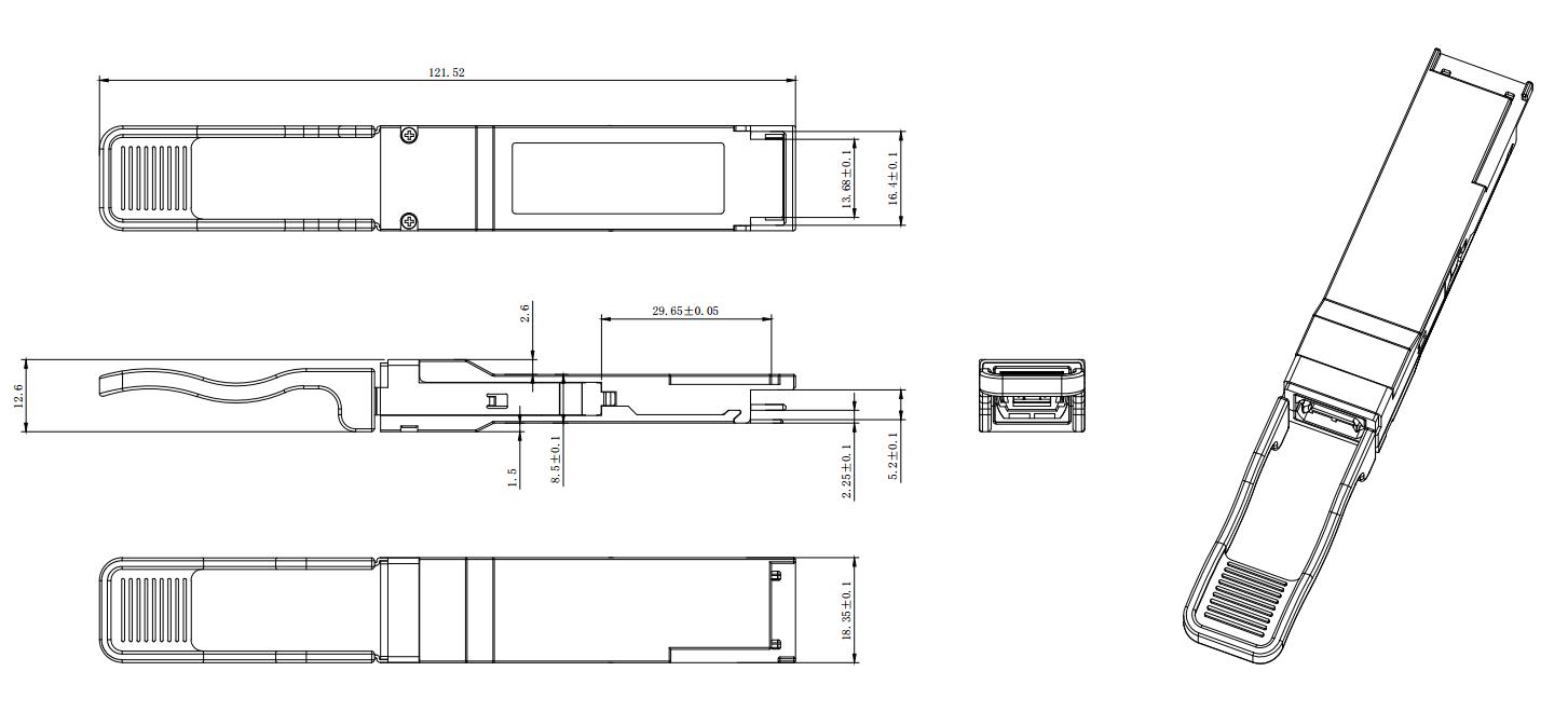
Ordering Code
|
Ordering Information |
|
|
Part Number |
Case Operating Temperature |
|
FTCQ-4X-PSMLR4-GC |
0 to 70 ºC |
|
FTCQ-4X-PSMLR4I-GC |
-40 to +85 ºC |
北亿纤通 | F-tone Networks
企业邮箱:该邮件地址已受到反垃圾邮件插件保护。要显示它需要在浏览器中启用 JavaScript。
企业手机:19081343401
企业电话:028-85255257
企业传真:028-85977702
注:本产品有全国产化型号可选
本产品为FT-WZ系列,仅展示部分参数,如有需要,请联系我们。
Important Notice
Performance figures, data and any illustrative material provided in this data sheet are typical and must be specifically confirmed in writing by F-tone Networks before they become applicable to any particular order or contract. In accordance with the F-tone Networks policy of continuous improvement specifications may change without notice.
The publication of information in this data sheet does not imply freedom from patent or other protective rights of F-tone Networks or others. Further details are available from any F-tone Networks sales representative.